What is moving of delay
- When designing synchronization, due to logical depth bias, several bottlenecks are generated. Sudden occurence of such bottleneck can greatly increase the setup time of FF and can lead to lowering of maximum opearting frequency many times.
- Here will assume that overalldesign has been accomplished with delay balance considered[1]and have recognized bottlenecks that could occur as a result of logical synthesis. Here will elaborate on method to easily adjust delay[2][3][4]without changing the logical description structure.
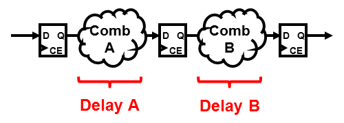
- See the pipeline below which joins combination circuit A and combination circuit B. Delay os system will assume as S so that Delay A��Delay S��Delay B.

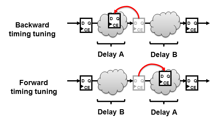
- Basic thinking is, to move the excess �� of delay A to fit inside the spare part of delay B. It is an extremely simple and easy thing, but how to design this using logic is the main point.

Application using change in description 1
- Although need to move FF that cuts off timing, it means that this will be supported by being in the combination circuit. When there is excess delay A and spare delay B, then description will be changed for circuit with excess delay A.

- For example, will assume that pipeline stage which latches 16 bit multiplication has excess delay. Signal a,b are FF output of prior stage and signal c is input to combination circuit of later stage.
always @(posedge clk)
        c[31:0]   <= #1 a[15:0] * b[15:0];
- Below as 16 bit into 16 bit multiplication is slow, 2 operations will be performed separately and then the results added (signal definition is omitted but although redundant, bit range is expressed) In this case delay adjustment will be as in the above diagram.
always @(posedge clk) begin
        c_h[31:8] <= #1 a[15:0] * b[15:8];
        c_l[23:0] <= #1 a[15:0] * b[7:0];
end

assign c[31:0] = {c_h[31:8], 8'd0} + {8'd0, c_l[23:0]};
- Former delay adjustment requires some manipulation in prior stage output FF. Actually, prior stage FF input signal aD, bD (D refers to D port input of FF), only remain and FF itself is removed. With this preparation, signal a,b �� signal aD, bD and become as follows
always @(posedge clk)
        c_h[31:8] <= #1 aD[15:0] * bD[15:8];
        c_l[23:0] <= #1 aD[15:0] * bD[7:0];
end

assign c[31:0] = {c_h[31:8], 8'd0} + {8'd0, c_l[23:0]};
- The above were intentionally separated into combination circuits, but there are many times when intermediate signal exists. In that case it is used as is.
Application using change in description 2
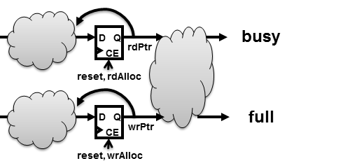
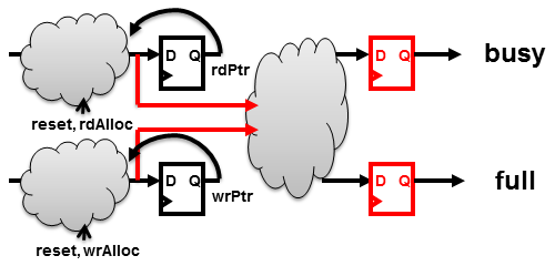
- Caution when using intermediate signal is, to use with same phase (position of stage), and to consider that the signal from D port of FF does not have CE port shape. For example, will assume that FIFO Busy and Full signals are defined as follows. Refer to FIFO Design example�iHowever rd and wr of signal name will be changed to i and o)
always @(posedge clk)
        if (reset)
                rdPtr[3:0] <= #1 4'd0;
        else if (rdAlloc)
                rdPtr[3:0] <= #1 rdPtr[3:0] + 4'd1;

always @(posedge clk)
        if (reset)
                wrPtr[3:0] <= #1 4'd0;
        else if (wrAlloc)
                wrPtr[3:0] <= #1 wrPtr[3:0] + 4'd1;

assign busy = (rdPtr[3:0] != wrPtr[3:0]);
assign full = (rdPtr[3]   != wrPtr[3]) & (rdPtr[2:0] == wrPtr[2:0]);

- It is combination circuit of Busy and Full, considering later factors will need to make delay 0 that is to say FF output. In this case will adjust prior stage delay.
// FF description wihout CE port
always @(posedge clk) begin
rdPtr[3:0] <= #1 rdPtrD[3:0];
wrPtr[3:0] <= #1 wrPtrD[3:0];
busy <= #1 busyD;
full <= #1 fullD;
end
// Transform to D type FF, and in case of system common reset, it is not required that reset signal be input.
// �iFor conveniently used D port is not required, but when replacing with above FF then reset is required.�j
assign rdPtrD[3:0] = reset ? 4'd0 : rdPtr[3:0] + rdAlloc;
assign wrPtrD[3:0] = reset ? 4'd0 : wrPtr[3:0] + wrAlloc;
// Genration of same phase Busy, Full for above D port.
assign busyD = (rdPtrD[3:0] != wrPtrD[3:0]);
assign fullD = (rdPtrD[3] != wrPtrD[3]) & (rdPtrD[2:0] == wrPtrD[2:0]);

- As mentioned above, by replacing signals which are used in assign descriptor for generating Busy,Full signals with D port input of FF at prior stage, can generate D port signals before making Busy, Full signals for FF�iGenerate instead of moving of FF�j�BOperation, result is identical for both.
- Here if signal other than D port is used then the pases will be strange and the operation will be wrong so must take care. Further, FIFO pointer rdPtrD and wrPtrD each must include reset and rdAlloc,wrAlloc being real FF D port signals. Very often, CE port of FF is overlooked.�iDescription without CE port.�j
Logical Circuit Design > Technic > �x���̈ړ� Next Page�iState Machine�j TOP of this page ��
